Termination in Transmission Line
The reflection Coefficient We will now state a basic principle. Any time a signal hits a junction of impedance change there is a reflection. The reflection coefficient is the ratio of the reflected voltage to the incident voltage. This ratio depends upon the impedances of the transmission line and the impedance of the junction. If a signal traveling on a transmission line of impedance Zo, hits an impedance Zt, the refelection coefficient is given by,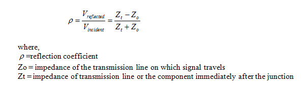
Example - A signal traveling on a transmission line of 50 Ohms has an amplitude of 3.3V. Find the magnitude of the reflected wave if the transmission line becomes thinner and the impedance changes to 60 Ohms.
Solution
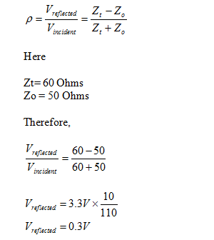
A voltage of 0.3V gets reflected at the junction. The positive value of the reflected voltage tells that the reflected voltage is a positive going pulse for a positive rising voltage.
Input Acceptance voltage
Let us assume that a step voltage V is impressed into a transmission line of characteristic impedance Zo. The source resistance of the drive signal is Rs. Assume that the transmission line is very long. So long so that, it will take few minutes for a small rise time signal ( say 100 ps) to travel from one end to the other. As soon as this signal crosses the resistor Rs, it sees an instantaneous impedance of Zo. The instantaneous voltage seen by the resistor and the transmission line junction is called input acceptance voltage.
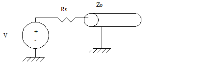
The transmission line in that case acts exactly like a resistor. The voltage impressed upon the transmission line is given by
Va = Vo Zo /( Rs + Zo)
The Source and Load impedance
The transmission line will eventually terminate to a receiver. The receiver can be though up of a differential op amp. The signal arriving at the receiver may or may not reflect from the receiver depending upon the load impedance. If the signal does reflect, it travels back to the source. At the source end it may again be reflected by the source depending upon the source impedance. The process continues to go on till the signal dies.
The process of the reflection determines the quality of the signal received at the receiver. We will try to see what termination strategies best gives out the signal received at the receiver.
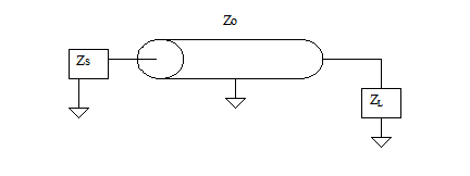
Figure The source and load impedance
Let us take a look at the figure above. Zs is source impedance and Zo is the characteristic impedance of the transmission line. The transmission line eventually terminates into load impedance ZL. Our problem is to determine the best possible source and load impedance values that creates best signal quality at the receiver end.
Let us assume A(w) is the input acceptance voltage. The input acceptance voltage is given by,
A(w) = Zo/(Zs+Zo)
The transfer function, which is the ratio of the voltage appearing at the load with respect to the impressed voltage is given by
S(w) = A(w)(1+ R2(w))/ [1-R2(w)R1(w)]
where,
R1(w) = Source end reflection function
R2(w) = Far end reflection function
We are ignoring the losses in the transmission line path.
The source and and far end reflection functions are given by,
R1(w) = [ZS(w)-Zo(w)] / [ZS(w)+Zo(w)]
R2(w) = [ZL(w)-Zo(w)] / [ZL(w)+Zo(w)]
The load impedance ZL(w) and the source impedance ZS(w) are the two factors that we can control to change the transfer function.
There are three basic ways to control the response function source termination, end termination and short line.
Source Termination
In source termination we set R1(w) to zero. This makes
S(w) = A(w)(1+ R2(w))
We note that the value of R1(w) is given by
R1(w) = [ZS(w)-Zo(w)] / [ZS(w)+Zo(w)]
Setting R1(w) to zero practically means setting the source impedance equal to the characteristic impedance.
Practically, in source termination, the signal travels down the cable, gets reflected from the load and travels back to the source ; but it does not reflect back from the source the second time.
With ZS(w) set to ZO(w), the input acceptance function has a value ½, which means that the amplitude of the signal traveling down the transmission line is one half he amplitude of the impressed signal. This seems to be a disadvantage of this method. The low voltage level is compensated by making the load impedance infinite or keeping it open (ZL(w) = infinity). This makes R2(w) = 1. The voltage reflected back from the load is doubled.
This methodology is used in PCI , PCI-X type of bus, where the voltage doubling is achieved at un terminated receivers.
End Termination
In end termination we simply set R2(w) = 0. This gives
S(w) = A(w)
The result of setting R2(w) to 0 is that it ends first reflection. The signal reaches the load and then there is no reflection.
Solving R2(w) = 0 gives ZL(w) = Zo(w). It means that we should set the load impedance same as the characteristic impedance.
Reflection from Capacitive Loads
When the signal reaches the destination, it will usually have additional capacitive load. Chip manufacturers often specify the capacitive load that may range form 5 pf to 20 pf. Let us take a look at the term for R2(w)
R2(w) = [ZL(w)-Zo(w)] / [ZL(w)+Zo(w)]
If ZL(w) is capacitive, its value will be negative( -1/jwC), R2(w) will have negative value which will imply that the reflected wave will have value inverse to that of the incidence wave.
Transmission Line An intuitive approach
As soon as the signal leaves the driver it sees an instantaneous impedance. If the impedance stays same it propagates without distortion. If there is a change in the impedance there is some reflection. The more the mismatch, greater is the reflection. If the impedance change is capacitive the reflection is negative. If the impedance change is inductive, the reflection is positive. Each and every change in the impedance during the flight time of the signal creates a point of discontinuity and therefore causes reflection and degradation of signal. This discontinuity can come in the form of change of layer, addition of via, addition of stub, change in trace width, to name some common form of changes.
From a PCB designer point of view, it is therefore of utmost important to keep the changes minimal during the time of flight of the signal on the PCB for a high speed design. Keep the number of vias minimum. Keep the layer changes to minimal. If there is a layer change, make sure that the characteristic impedance stays constant as it changes layers. The change in the trace width should be used only in the break out region, where it is impossible to route traces using wider traces.
Previous - Compensating Discontinuity Next - Transmission Line Losses