Impedance Calculator in PADS PowerPCB
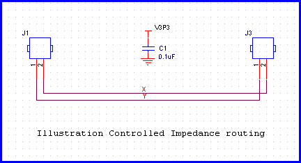
Most of the modern layout tools have ability to calculate the impedance as a part of the software. We will present here an impedance calculation method using PADS router. Let us try to create a schematics with two simple traces as shown below. The net names of these traces are X and Y. It is required that these traces have impedance of 55 Ohms.
A quick calculation using formula method from http://referencedesigner.com/tutorials/si/si_06.php shows that the following arrangement achieves 55 Ohm impedance.
Width of trace = 10 mils
Er = 4.5
Height above ground = 7 mils
We have assumed the trace thickness to be 1 mils. A 1 oz trace has thickness of 1.35 mils. But we want to keep the things simple, so 1 oz is good enough for our understanding.
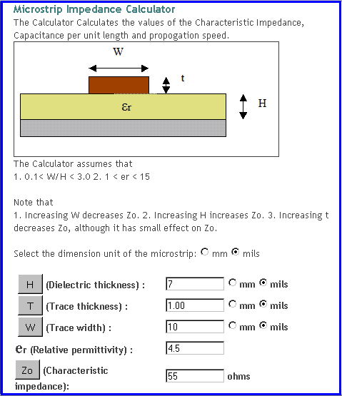
Figure 9.7 - Calculating the impedance from formula using online calculator.
Now let us set the layer stack up in PADS PowerPCB as follows.
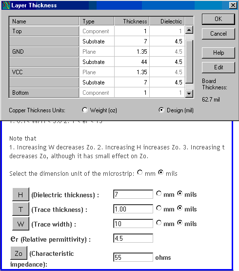
Figure 9.8 - Setting up layer stackup in PADS PowerPCB.
In order to check the Impedance and to see if any trace violates the impedance rule we set the rules for impedance as follows. Click on Setup -> Design Rules -> Nets-> Select the nets X and Y-> High Speed. You should be able to see something similar to the figure below.
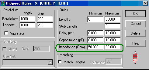
Figure 9.9 - Setting the Impedance limits for High Speed nets.
Now we will route the net X with width 10 mils as calculated. We will route net Y with width 20 mils deliberately creating error. Here is how the routed PCB looks like.
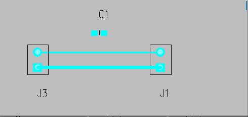
Figure 9.10 - Routed PCB with one trace 10 mils and other trace 20 mils.
We can use the high speed verification tool of PADS to check the impedances of the individual routed nets. Click on Tools -> Verify Design -> High Speed. Click on Setup and check impedance. Click Parameters and uncheck Report Violations Only. Click ok to close the EDC parameters Window. Click ok to close the Electrodynamic check Window. Now hit start to run the High Speed Design Rules. You will notice that it reports violation for the 20 mils trace.
If you hit the view report you should be able to see something similar to the below.
ELECTRODYNAMIC CHECKING REPORT -- DESIGN10.pcb -- Fri Sep 12 17:45:46 2008

Check net: X

Linear parameters checking.

Length  Capacitance  Impedance   Delay( J1.2 - J3.2)
   824   2.25(pF)   55.8  55.8      0.125(ns)

Net X  is daisy chained

Check net: Y

Linear parameters checking.

Length  Capacitance  Impedance   Delay( J1.1 - J3.1)
   824   3.48(pF)   37.3  37.3      0.130(ns)
                     Violated

Net Y  is daisy chained
The PADS Electrodynamic test reports an impedance of 55.8 Ohms for the 10 mil trace. This is fairly close to the formula method reported above. For the 20 mils trace, it reports an impedance of 37.3 Ohms. Since this is out of the specification 50 to 60 Ohms it reports error.
Most commercial routing tools have inbuilt impedance checking method. We should take advantage of these to check for any possible violation. It is important to note that we should define the stackup and its cross section early in the PCB design stage.
Previous - Impedance Calculator for Microstrip Next - IPC, Wadell and 2D solver comparison