Compensating small Inductive or Capacitive discontinuity
In the transmission line it is not always possible to maintain the required impedance along the complete path of the transmission line. If the discontinuity is capacitive, there is a negative reflection. If the discontinuity is inductive, there is a positive reflection. If the delay corresponding to the continuity is small, in the range less than one third of the 10% to 90% rise time of the signal, a capacitive discontinuity can be overcome by including a matching inductive discontinuity. The negative reflection from the capacitive discontinuity is matched by the positive reflection from the inductive discontinuity. In a similar way an inductive discontinuity can be overcome by including a matching capacitive discontinuity. The positive reflection from the inductive discontinuity is matched by the negative reflection from the inductive discontinuity.A trace can be made more inductive by reducing the width of the trace. The length and amount of the reduction should be such that the overall impedance seen by the transmission line stays constant.
To see the effect of the discontinuity compensation, let us take a look at the following hspice code.
*Capacitive Discontinuity
.PARAM impedance =  50
.OPTION Post Probe
.Tran 50ps 6ns
VIN 1 0 PWL 0 0v 50ps 0v 350ps 3.3v
Rsource 1 2 50
T1 2 0 3 0 ZO=50 TD=1000ps
T2 3 0 4 0 ZO=impedance TD=100ps

C1 4 0 1.5p

T3 4 0 5 0 ZO=impedance TD=100ps
T4 5 0 6 0 ZO=50 TD=1000ps
.Probe v(1) v(2)v(3)v(4)v(5) v(6)
.End
This is a simple source terminated, reflected wave topology. We have 4 transmission line sections. Two of them are before the capacitive discontinuity and two of them are after the capacitive discontinuity C1.
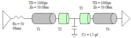
Figure A capacitive discontinuity in transmission line.
The transmission line before the capacitive discontinuity has been broken into two parts T1 and T2. The second part T2 is a small section of the transmission line, which we will use to create a inductive transmission line to partially offset the effect of the capacitive loading. Similarly, the transmission line after the capacitive loading has also been split in two parts T3 and T4. The part T3 will be used to partially offset the capacitive discontinuity.
Here is the simulation result when all four sections of the transmission lines are of same impedance, Zo = 50 Ohms.
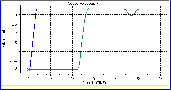
Figure - Reflections from Capacitive discontinuity
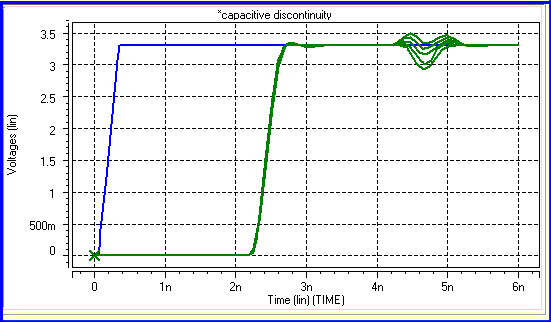
In order to reduce the capacitive discontinuity, we will make the two small transmission lines around the capacitor to have impedance higher than 50 Ohms. By doing so, we make it inductive. We can think of this thin transmission line to have excess inductance. This excess inductance partially balances the excess capacitance. We now run the simulation for the values of impedances of 50 Ohms to 70 Ohms in steps of 5 Ohms to see its effect on the reflection.
We use the hspice sweep to accomplish this task. The statement
.Tran 50ps 6ns SWEEP impedance 50 70 5
varies the value of impedance from 50 to 70 in steps of 5.
Here is the result of the simulation.
Calculating the length of the thin trace.
The possibility of the creating a thinner trace on the PCB to counter a shunt lumped capacitor exists only if the trace widths for nominal 50 Ohms trace is greater than the minimum allowed PCB trace width. If for example the trace width is 5 mils to achieve the required 50 Ohms impedance and manufacturing house does not allow traces smaller than 4 mils, there is probably no good chance of creating a low inductance trace to match the shunt lumped capacitor.
It is important to note that we should select the thinnest possible trace to compensate the capacitive loading. The thinner the trace, the smaller will be the required length of the trace. The rise time corresponding to the thin section of trace should be small in comparison to the rise time of the incident trace.
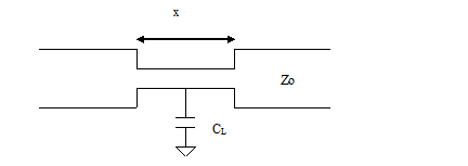
Let us assume that the x is the length of the thin section of the PCB trace used to match a capacitive load CL. The characteristic impedance of the normal trace is Zo.
If L1 is the inductance per unit length and C1 is the capacitance per unit length of the thin section of trace then,
Inductance of the thin section of trace = xL1
Capacitance of the thin section of trace = xC1
If Z1 is the characteristic impedance of the thinner section of transmission line, then
L1 = Z12C1 The impedance of the thin section of the trace along with the load capacitor CL is given by
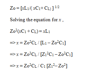
This equation can be used to calculate the length of the transmission line required to match the capacitive discontinuity. Here are the steps involved
1. Find the width of the thinnest possible trace.
2. Calculate the capacitance per unit length and impedance of the thin section of the trace
3. Calculate the length of the thin section of the trace.
4. Find the delay of the thin section of the transmission line and ensure that the incoming signal rise time is at least three times larger than the time corresponding to this delay of the thin section of the transmission line.
5. Verify the signals using simulations.
We will use an example to illustrate this theory. Assume that we have a 4 Layer stackup. The trace width is 10 mils and the height above the ground plane is 7 mils. The dielectric constant is 4.3. The hspice code to generate the rlgc matrix is given below.
* W element, field-solver interface

*                  XXXXXX
*  ------------------------------------ Z = 8mils
*       Er = 4.3   H = 7mils
*  ------------------------------------ Z = 1mils
*  //// Bottom Ground Plane ///////////
*  ------------------------------------ Z = 0

W1 in1   0 out1   0 FSmodel=demo N=1 l=0.97

* Materials
.MATERIAL copper METAL CONDUCTIVITY=5.76e+07
.MATERIAL diel_1 DIELECTRIC ER = 4.3  LOSSTANGENT=1.2e-3 CONDUCTIVITY=8.2e-4

* Conductor crossection shapes
.SHAPE rect RECTANGLE WIDTH = 10mils HEIGHT = 1mils

* Dielectric stack-up
.LAYERSTACK Stack
+ LAYER = (copper, 1mils)
+ LAYER = (diel_1 7mils)

* Field-solver options
.FSOPTIONS myOption ACCURACY = LOW GRIDFACTOR = 1
+ ComputeRo=no ComputeRs=no ComputeGo=no ComputeGd=no PRINTDATA=YES

.MODEL demo W ModelType=FieldSolver
+ LAYERSTACK=Stack FSOptions=myOption
+ RLGCFILE= rlgc.txt
+ CONDUCTOR = ( MATERIAL=copper, SHAPE=rect, ORIGIN=(1000mils, 8mils) )
*Analysis
.tran 0.1ns 100ns
.option post
.end
*SYSTEM_NAME : demo
*
*       Half Space, AIR
*  ------------------------------------ Z = 2.032000e-004
*       diel_1   H = 1.778000e-004
*  ------------------------------------ Z = 2.540000e-005
*  //// Bottom Ground Plane ///////////
*  ------------------------------------ Z = 0

* L(H/m), C(F/m), Ro(Ohm/m), Go(S/m), Rs(Ohm/(m*sqrt(Hz)), Gd(S/(m*Hz))

.MODEL demo W MODELTYPE=RLGC, N=1
+ Lo = 3.357079e-007
+ Co = 1.004718e-010
The characteristic impedance corresponding to these values of Lo and Co is 57.8 Ohms. The minimum allowed trace width for the PCB is 4 mils. We can calculate the characteristic impedance and capacitance per unit length of the 4 mils trace by changing the statement in the spice code from
.SHAPE rect RECTANGLE WIDTH = 10mils HEIGHT = 1mils
to one with
.SHAPE rect RECTANGLE WIDTH = 4mils HEIGHT = 1mils

This produces the following rlgc matrix.

*SYSTEM_NAME : demo
*       Half Space, AIR
*  ------------------------------------ Z = 2.032000e-004
*       diel_1   H = 1.778000e-004
*  ------------------------------------ Z = 2.540000e-005
*  //// Bottom Ground Plane ///////////
*  ------------------------------------ Z = 0

* L(H/m), C(F/m), Ro(Ohm/m), Go(S/m), Rs(Ohm/(m*sqrt(Hz)), Gd(S/(m*Hz))

.MODEL demo W MODELTYPE=RLGC, N=1
+ Lo = 4.770826e-007
+ Co = 6.549558e-011
The impedance corresponding to these values of Lo and Co is 85.34 Ohms. Let us assume that the capacitive discontinuity has a value of 2 pf.
Using the formula
x = Zo2CL / C1 [Z12 Zo2]
We have
Zo = 57.8 Ohms
Z1 = 85.34 Ohms
CL = 2 pf = 2x10-12 faraad
C1 = 6.54955810-11 farad /meter
Substituting these values give
x = 0.02587 meter or 1.0811 inches
The delay corresponding to the thin section of this transmission line is 145 ps.
Let us create some spice simulation to the effect of the capacitive discontinuity and the use of this equation. The spice code to do the simulation is given below.
* Calculation of thin trace length in capacitive reflection
.Tran 50ps 8ns sweep thin_trace_impedance 57.8 85.3 27.5
.OPTION Post Probe
VIN 1 0 PWL 0 0v 50ps 0v 550ps 3.3v
Rsource 1 2 57.8
T1 2 0 3 0 ZO=57.8 TD=1000ps
T2 3 0 4 0 ZO=thin_trace_impedance TD=74ps
C1 4 0 2pf
T3 4 0 5 0 ZO=thin_trace_impedance TD=74ps
T4 5 0 6 0 ZO=57.8 TD=1000ps
.Probe v(1)v(6)
.End
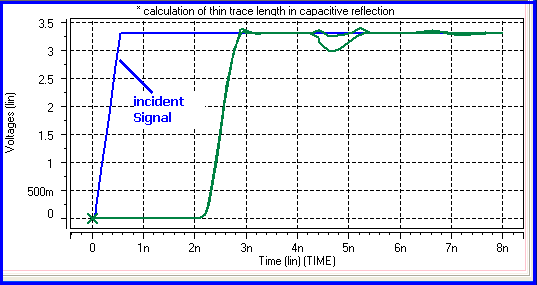
Figure - Effect of thin trace on capacitive reflection.
The incident signal has been modeled as a piecewise linear signal with 0 to 3.3V time of 500ps. This is slightly more than the thrice the time of the thin section of the transmission line which we have calculated as 145 ps.
We see that the reflections from due to the capacitor is considerably reduced by the thin traces.
Thin Traces at breakout region
A breakout region has thin traces because of the space limitation. The thin traces lead to the increase in impedance and an inductive reflection. The polarity of this reflection is in the same direction as that of the incident signal. If the length of the thin trace is small less than one third that of the rise time of the incident signal, the inductive discontinuity can be overcome by a small length of wide trace. In such case, negative reflection by the capacitive effect of wide trace balances the inductive reflection from the thin traces.
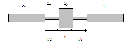
Figure Matching thin trace with wide trace to minimize inductive reflection
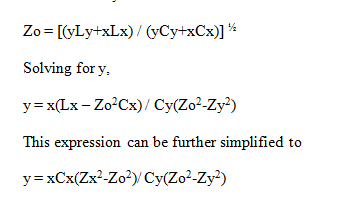
Let us assume that the thin trace has a length of x and has Characteristic impedance Zx and capacitance per unit length of Cx. We want to match it with wider trace having characteristic impedance of Zy and capacitance per unit length of Cy. We want to find the length of the trace segment y. If Lx and Ly are inductances per unit length of thin and wide sections respectively, then the impedance of the two sections combined should match the characteristic impedance Zo. We can express this relation mathematically as
Previous - Capacitive Discontinuity Next - Compensating Discontinuity