Surface Dielectric and Radiation Losses
Effect of Surface Roughness on Signal LossThe PCB surface is not perfectly smooth. When observed under microscope, they show surface roughness similar to the figure shown below. The surface roughness is measured by the distance between the peak and the valley of the tooth like structure of the PCB trace. In a typical PCB they have dimensions of the order of 0.3 mils.
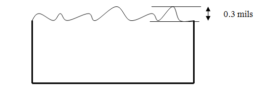
Surface roughness of a typical microstrip
If the frequency of the signal propagating through the trace is low, the surface roughness has no effect on the signal. At low frequencies, there is no skin effect and the current flows uniformly through the section of the PCB trace. As the frequency of the signal is increased, the skin depth of the signal reduces. When the skin depth is less than dimensions of the surface roughness, most of the current flows in a roller coaster form along the rough surface of the PCB trace. This effectively increases the distance that the current needs to travel and therefore there is an increase in the resistance of the PCB trace.
The surface roughness becomes noticeable beyond 1 GHz frequency. If your design contains frequencies in the vicinity of 1 GHz, it has significant trace length on the PCB and if the signal at receiver is sensitive to the losses in the path, you must take into account the additional skin loss effect due to the surface roughness.
Dielectric Losses
Dielectric loss results from the heating effect on the dielectric material between the conductors. When a signal is propagating around a dielectric, a part of the signal is consumed in heating up the dielectric material resulting in the signal attenuation. The heat absorbed is directly proportional to the dielectric loss factor for that material. Dielectric loss is also a function of frequency. The FR-4 material commonly used in printed circuit boards has negligible loss below 1 GHz. As frequency goes above 1GHz, the dielectric loss increases. We can also understand the dielectric loss phenomenon from atomic structure point of view. In the absence of potential difference between two conductors, the atoms in the dielectric material between them are normal. The orbits of the electrons are circular. When a potential difference is applied between two conductors, the orbits of the electrons change. The negatively charged conductor repels the electrons of the dielectric atom towards the positively charged conductor. A movement in the path of electrons takes its energy from the applied voltage source. This causes the signal to get attenuated.
Radiation and Induction Losses
When the conductor carrying a high frequency component has a nearby conductor or metallic object, a current is induced in that object. This results in power being dissipated in the object. This ultimately causes the propagating signal to attenuate.
There can also be radiation losses which happens when the magnetic lines of force for not return to the conductor. The lines of forces are projected into space as radiation it results in attenuation to the signal propagating through the wire.
To reduce the Induction loss we must minimize any presence of nearby conductor. This not only reduce induction loss, but also reduces the crosstalk in the nearby conductor. To minimize the radiation loss we must ensure that the characteristic impedance stays constant through out the path of the transmission line and there is proper load matching scheme.
Previous - Skin Effect Next - Chapter 9 - Question and Answers