Reflections from Capacitive Discontinuity
In PCB designs, the shunt capacitance in the path of a trace can be created by via, pads, test points. It may also be created if a circuit has daisy chain connection creating a load in the middle of a transmission line.When a signal propagating on a uniform transmission line encounters a shunt capacitance in its path, a signal is reflected. The polarity of the reflected signal is opposite to that of the incident signal.
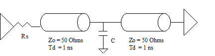
Figure - A capacitive discontinuity in a transmission line.
There are three factors that govern the amplitude of the reflected wave signal. The magnitude of the capacitance, the rise time of the signal and the impedance of the transmission line.
Effect of Incident Signal Rise time
The magnitude of the reflected wave is more for incident wave with smaller rise time. In the above figure let us assume a driver with 50 Ohm source termination driving a 50 Ohm transmission line. Let us try to see the effect of the rise time on the shape and magnitude of the reflected wave due to the capacitor.
Here is the code for an hspice simulation showing the magnitude of the reflected wave as a function of the rise time.
* Example of parameter sweep
.PARAM risetime =  250ps
.Tran 50ps 8ns sweep risetime 150ps 550ps 100ps
.OPTION Post Probe
VIN 1 0 PWL 0 0v 50ps 0v risetime 3.3v
Rsource 1 2 50
Tfirst 2 0 3 0 ZO=50 TD=1000ps
C1 3 0 1.5p
Tsecond 3 0 4 0 ZO=50 TD=1000ps
.Probe v(1) v(2)v(3)v(4)
.End
In this code we are trying to sweep the value of variable risetime. Its value changes from 150 ps to 550ps in step of 100 ps. This is accomplished using the statement
.Tran 50ps 8ns sweep risetime 150ps 550ps 100ps
This sweep is used to generate a voltage source. The rise time of the voltage source varies from 100ps to 500 ps in steps of 100ps. This is accomplished using the statement
VIN 1 0 PWL 0 0v 50ps 0v risetime 3.3v
If we simulate using the above code we get a graph similar to the one shown below.
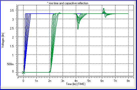
Figure - Effect of rise time on Capacitive reflection.
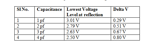
Here is the table enlisting the value of the local voltage minima corresponding to the reflection at the capacitor and the value of the height of the voltage reflection.
Table Variation of the reflected wave amplitude with incident signal rise time

We also observe that as the rise time of the incident wave increases, the width of the reflected signal increases.
Effect of the Capacitance Value on reflection
As the value of the capacitance increases, the magnitude of the reflected signal increases. Let us see this effect in hspice simulation. The following the hspice code that varies the value of the capacitance from 1pf to 4pf, for a signal with rise time of 300ps.
* Cap value and capacitive reflection
.PARAM cap_value =  1pf
.Tran 50ps 8ns sweep cap_value 1pf 4pf 1pf
.OPTION Post Probe
VIN 1 0 PWL 0 0v 50ps 0v 350ps 3.3v
Rsource 1 2 50
Tfirst 2 0 3 0 ZO=50 TD=1000ps
C1 3 0 cap_value
Tsecond 3 0 4 0 ZO=50 TD=1000ps
.Probe v(1) v(2)v(3)v(4)
.End
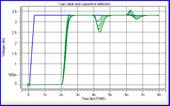
Effect of capacitance on capacitive reflection.
The table below shows the variation of the voltage with capacitance value.
Table Effect of capacitance on the magnitude of reflected voltage
Effect of Impedance on Reflection
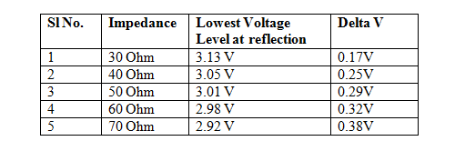
As the value of the impedance of the path increases, the magnitude of the reflected signal from capacitive discontinuity increases. Actually the amount of the reflection depends upon the ration of the incident transmission line impedance and the magnitude of the capacitive impedance. The larger is this ratio, the more is the magnitude of the capacitive reflection. Let us see this effect in hspice simulation. The following is the hspice code that varies the value of the impedance from 30 Ohms to 70 Ohms, for a signal with rise time of 300ps. The value of the capacitance in the capacitive discontinuity has been assumed to be 1pf.
* Impedance and capacitive reflection
.PARAM impedance = 50
.Tran 50ps 8ns sweep impedance 30 70 10
.OPTION Post Probe
VIN 1 0 PWL 0 0v 50ps 0v 350ps 3.3v
Rsource 1 2 impedance
Tfirst 2 0 3 0 ZO=impedance TD=1000ps
C1 3 0 1pf
Tsecond 3 0 4 0 ZO=impedance TD=1000ps
.Probe v(1) v(2)v(3)v(4)
.End
If we run the above code, we get a signal similar the one shown below
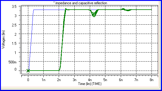
Figure Effect of Impedance on magnitude reflection.
The table below shows the variation of the reflected wave amplitude with impedance value.
Table - Impact of Impedance on reflection
We have seen that whenever there is a capacitive discontinuity there is a reflection. This reflection degrades the signal quality. The capacitive discontinuity can be caused by via, a thick trace, a test point, a multi drop daisy chain routing. The reflection can also be caused by inductive discontinuity. A thin trace or a connector cause inductive discontinuity.
Whether it is capacitive discontinuity or an inductive discontinuity, it eventually leads to degradation in signal at the receiver. As a PCB designer we must be aware that we take precautions to create as small discontinuity during the time of flight as possible.
Previous - Impedance between Power Planes Next - Compensating Discontinuity