Routing Differential Signals on PADS Router
It is worthwhile to take a look at how we can successfully route a differential signal with a commercial auto router such as PADS Router© (earlier PADS PowerPCB©). Our purpose is to route successfully, the circuit shown below.
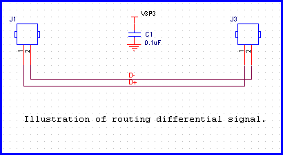
Figure 8.4 - A Schematics for illustrating routing differential signal in PADS
J1 and J3 are the two connectors that connect two differential signals. C1 is a decoupling capacitor. For the purpose of learning we will design a 4 Layer PCB stackup. The PCB stackup is as follows
Layer1
GND
VCC
Layer2
We need to maintain a 100 Ohms differential impedance. The best way to calculate the single ended or differential impedance is to use a 2D field solver which will give accuracy to the range of 1 or 2%. However, I assume that we do not have the access to the 2D field solver and we will use formula method (you can use the website http://referencedesigner.com/tutorials/si/si_06.php to calculate the single ended impedance) to calculate the single ended and then differential impedance. Using the formula we get the following values for a single ended impedance of 55 Ohms
Trace width = 10 mils
Thickness of Dielectric = 7 mils
Trace thickness = 1.0 mils
Er = 4.5
This gives characteristic impedance of single ended trace as 55 Ohms. Our stack up has a separation of 0.007 between top layer and Ground layer as also between bottom layer and VCC Layer. The separation between the Power and ground layer is 0.044. If we take into account thickness of the soldermask and the copper layers as 0.005 in total, it roughly makes up 0.063 of board thickness.
Let us now calculate the differential impedance. We will again use the formula method instead of the 2D field solver. We must bear in mind that the 2D field solver will give better accuracy. But this method should work as well for the purpose of learning. As an example using the calculator at http://referencedesigner.com/tutorials/si/si_10.php we get the following result.
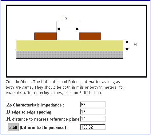
Figure 8.5 Calculation of Differential Impedance using online Calculator
Notice that in the above case we get 100 Ohms for 18 mils separation between the + and traces and 10 mils separation from the ground trace. We will adjust the separation between the trace and the required height to achieve 100 Ohms. For, 7 mils separation between the trace and ground layers, the separation between traces will have to be lesser to achieve 100 ohms. We will now see how to implement it in PADS router.
The netlist is imported in PADS. The layer assignment looks as follows
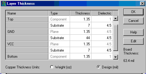
Figure 8.6 Setting up layer stack up in PADS Layout
In order to successfully route the signal we should define the design rules. To do that click on Setup -> Design Rules -> Differential Pairs. You should be able to see something similar to the figure 8-7.
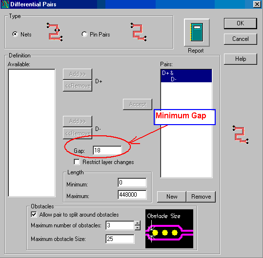
Figure 8.7 Defining differential pair in PADS router.
We should also define some more rules. These are the trace width of these traces have to be exactly 10 mils. Secondly the length matching of these two traces should be set at 50 mils. The trace width can be set to 10 mils using Setup -> Design Rules -> Net -> Select the nets and click clearance. We should also set the net to net trace width to be 18 mils (as an example) for the differential traces. The trick is that while routing we will keep the DRC (Design Rule Check) ON. We will then try to route the traces as close together as possible. When we try to reduce the separation below 18 mils, the router will not allow us to do so. We will therefore be routing with separation between the traces as 18 mils.
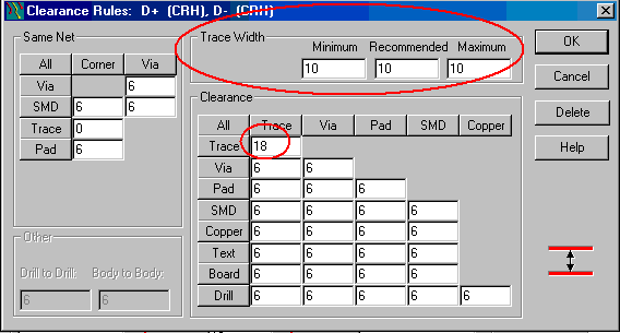
Figure 8.8 Setting trace width and trace separation in PADS
The length matching can be forces to be set as follows. Note that we have also set the impedance requirement to be between 50 Ohms to 60 Ohms.
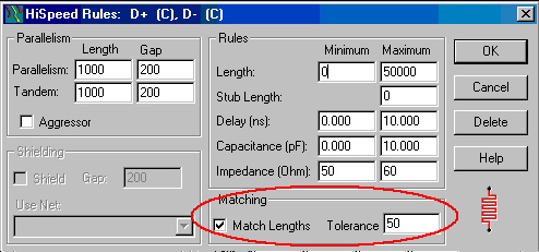
Figure 8.9 Setting Length matching of differential pair
We are now all set to start routing. PADS uses altium design rules to check the differential traces. You can now check if the differential traces follow the design rules.
Previous - HyperTransport Differential Bus Impedance Calculator using Hspice 2D