Bypass Cap, Local Capacitor
7.6 Series Inductance of Bypass Capacitor and need for local capacitor.Every capacitor has a series inductance. A capacitor can therefore be modeled as a capacitors in series with an inductor and a resistor. When the frequency of noise element increases, the effective AC impedance of the capacitor increases. The capacitor is no more able to shunt the AC noise to ground. You can view the inductor as in need of being charged and not allowing the ac voltage to go to ground.
To overcome this problem, we use a number of small capacitors. These capacitors are placed very close to the power supply pins of ICs to keep the inductance very low. They should be routed with wide trace.
7.7 Find the Impedance profile of power supply
As a PCB designer you do not have time to calculate the number and required quantity of capacitors. But you can do it if you want to. Before I explain how to do it, I would like to you to do an exercise. I want you to plot the impedance profile of the your power supply at all frequency. You already have done few PCB designs. Grab the schematics of one of the designs you have done. Find one particular power supply net and list out all the capacitor on this net. There will be couple of electrolytic capacitor. There may be some plastic film capacitor. And there may be a large number of small ceramic capacitor (0.1uF or 0.1uF). Make a list of all of them. Write down the part numbers of these capacitors and their quantity in the design. Now download the datasheets of all of them. From their datasheets, find the value of the Effective Series Resistance and Effective Series Inductance of the capacitors. If these values are not mentioned in the datasheets, try to make intelligent guesses from similar capacitors. Derate the inductance value a little bit to take into account the mounting trace inductance.
Once you have done that enter them in an spread sheet. An example of such a spread sheet is shown below.
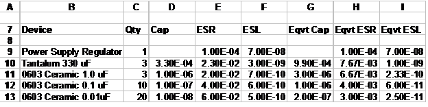
The power supply regulator has its own series resistance and effective series inductance, which will depend upon the length of the wire from the power supply regulator IC to the power planes. The values ion column D, E and F for the capacitor are taken from the datasheet of the components. The values in columns G, H and I are the equivalent capacitance, equivalent resistance and equivalent inductances. For example the equivalent capacitances of 10, 0.1 uF capacitors is 1 uF. The equivalent inductance of 20 0.01 uF capacitors with 0.5nH inductance each is .025 nH. The equivalent capacitance increases and equivalent inductance and equivalent resistance decrease.
With the equivalent capacitance, equivalent ESR and equivalent inductance, we can find the impedance of each set of capacitor using the formula
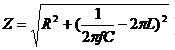
We now extend the spread sheet to list the impedance of the each set of the capacitors at different frequencies.
The total impedance is calculated using the formula
1/Z = 1/Z1 +1/Z2 +1/Z3 + ......
This way we can find the impedance of our impedance at different frequencies. As an example, in the above case, the total impedance at 10 MHz is 0.0052. The impedance at 500 MHz is 0.05 Ohms.
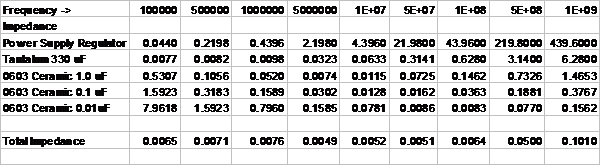
We can also plot the curve of the variation of the impedance with frequency. We can then see which frequencies have higher impedance. We can then adjust the number of capacitors or the values to ensure that the impedance stays lower that the value required.
Figure 7.4 Variation of Impedance with Frequency
Before we proceed further, we would also like to take into account the capacitance of the power and ground plane. We will see later that the power and ground plane capacitance play an important role.
7.8 Capacitance of Power-Ground Plane
If the Power and Ground planes are routed adjacent to each other, they act as a parallel plate capacitance. Since there is no lead, they do not suffer from effective series inductance as in normal capacitors. Therefore they are effective for high frequency ranges.
The capacitance of a parallel plate capacitor is given by
C = εoεrA/d [7.7]
where,
εo = 8.87x10⁻¹² Nm2/C2
εr = relative electric permeability of the dielectric
A = Area formed by the ground and power plane.
d = separation between the power and ground plane.
The above formula is for metric units. If you would like to work in inches ( as is the case for PCB designs), you can use the formula given below
C = 0.225 A/d [7.8]
Where A is the area in square inches and d is the separation between ground and power plane in inches.
Previous - How to achieve low impedance Next - Tom-bob-Ch7