Timing Relationship between Signals
CHAPTER 22 Timing Relationship between Signals
If you have already designed some high speed PCBs or if you have been involved in some way in high speed PCB design, you must have come across design rules that require the difference in the length of the PCB trace to be within a specified limit.
These rules are often results of the relation between the clock and data signal timing. There is a timing window in which the data must arrive at the rising edge or falling edge of the clock. If the data arrives too early and goes away or if it arrives too late it is of no use.
Let us take some time to understand the concept of the setup and hold time and see how we can ensure its proper implementation at the PCB level.
2.1 Setup and Hold Time
The concept of setup and hold time can be best understood with the picture shown below.
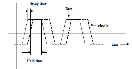
Figure 2 1 - Illustration of set up and hold time
The curve shows a clock and a data signal. The data signal latches at the rising edge of the clock. The clock signal is in dotted line and data signal is in solid line.
Set up time is the amount of time before the clock edge that the input signal needs to be stable to guarantee it is accepted properly on the clock edge. Hold time is the amount of time after the clock edge that the same input signal has to be held before changing, to make sure it is sensed properly at the clock edge.
Setup and hold times are vigorously simulated at the chip design level to ensure that they meet the specification. As a PCB designer our job is to make sure that we do not deteriorate them as the clock and data signals propagate along the PCB.
Let us assume that IC A is the source of a clock and a data signal. The IC B is the destination of the clock and the data signal. In its simplest form usually the clock and the data signals will have their length matched and there will not be any change in the setup time when the signal leaves IC A to when it reaches B. If however, the length of the clock signal is much smaller than the length of the data signal on the PCB, the data will arrive too late. The setup time margin will get reduced as the data signals reach IC B.
Whether this will cause any failure or not will depend upon edge rate, clock frequency the setup time specification of the IC B. For example for a clock source of 1 MHz frequency and slow edge rate we know pretty much sure that it will not create a setup time violation with normal PCB sizes. For 100 MHz clock source we would like to do a quick calculation as to how much mismatch is allowed. For 1 GHz clock and fast edge rates we must do calculation and take special cares as dictated by the bus technology and the setup time requirements of the destination IC.
Previous -Tom and Bob- Chapter 1 Time and Distance