PCB Design for High Speed
CHAPTER 11.6 PCB Design for High Speed
As a PCB Designer you need to alter your habits a little bit, if you want your board to work for high speed.
As soon as you receive the board from the designer you need to stop and spend some time on the signal integrity aspect of the design. This may mean that you will have to spend some extra time on your already long list of tasks of creating footprints, maintaining library, doing placement, doing routing, maintaining revisions, generating gerber files and creating documentation. But if your design has high speed signals you have no option but to adhere to at least some of the basic rules.
As soon as you receive the designed schematics, go through the schematics and note down all the nets that need special signal integrity concern. It will be better if you get involved in the early design stage. This can be done by studying the block diagram of the design and by reading about the major ICs used the design. If the design involves, say, for example DDR3, spend some time to read about DDR3. Note down the timing considerations and relative timing requirements between clock and data lines, between data strobe and data lines. If your layout tool has the ability to automatically generate DRC (Design Rule Check) errors based upon the length or timing difference between traces, learn how to implement it. Learn by experimenting draw a simple circuit with jut 3 or 4 nets and find how to implement relative timing or distance constraints between traces or nets.
If your layout tool does not possess capability to enforce length matching, learn how to generate a length report. Learn how to use the length report to implement timing and relative length constraints. Sometimes, using a script is a faster way to check the length constraints. You should also make a checklist that will list all the critical nets. The checklist will have checks for length constraints.
You will also study the schematics to find the most critical nets. You will place the components in such a way that it minimizes the length of the high speed nets. If there are two ways to place components, prefer the one that reduces the routing length of the high speed nets.
Most of the high speed nets are required to have a definite value of characteristic impedance (typically 50 O). This definite value of characteristic impedance is achieved by routing the signal with a precise value of this width of the signal (5 mils is a typical value) and its separation from the ground and power planes. As soon as you have the schematics ready, you will identify all the nets that need a definite desired value of characteristic impedance. Power nets are not part of the nets requiring definite value of characteristic impedance they are usually routed with wider thickness. As a first approximation, use online calculators to find the desired width of high speed traces for given trace plane separation. Find out if your layout tool has inbuilt 2D field solver to calculate the characteristic impedance. If it has, learn how to use it to calculate the characteristic impedance.
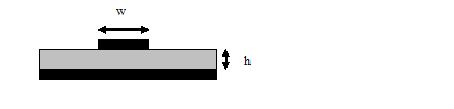
Figure 1.1 The characteristic impedance of a microstrip is close to 50 O if w=2xh
Based upon the desired value of the characteristic impedance, you will design a stackup. The stack up will be designed such that it will satisfy the characteristic impedance requirement for all the layers on which you intend to route high speed signal. The stack up will be designed such that it will provide proper return path for high speed signals. If there are more that one power islands in the power layer, they should be connected by stitching capacitor to provide continuous path for return signal. The stackup will preferably have power and ground plane adjacent to each other for providing adequate capacitance between power and ground plane for very high frequency decoupling.
Most of the todays designs have large number of differential signaling traces. You will identify all the differential nets in your design. All differential signals are required to have a definite value of differential impedance. To achieve the required differential impedance, you will need
1. definite value of width of trace
2. definite value of separation between the positive and negative trace.
3. definite value of separation between the trace and power or ground layers.
You will also have to keep the lengths of the positive and negative traces matched, typically within 50 mils. Most layout tools now a days have support for differential signaling. If you have not explored, it is time to learn the capabilities of your layout tool for routing differential signaling.
A number of discrete components in the schematics are required for maintaining the integrity of high speed signals. This includes series terminating resistors or end terminating resistors. Their placement is crucial for achieving integrity of the signal. You will study the schematics to identify all discrete components in the path of the high speed signals and find their desired placement. A series source terminating resistor, for example, is required to be placed very close to the driver. You will study all the constraints and implement them is your layout constraint. A separate check list should be maintained which should be checked and completed before the design is signed out.
Placement of capacitors close to the ICs is crucial to achieve noiseless power supply. The traces from the power and ground ends of the capacitor should be thick. The vias for power and ground traces should be large. The traces connecting the power and ground vias should be close.
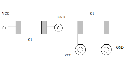
Figure 1 2 Two methods of routing power and ground traces from a power supply decoupling capacitor. The second one is better because, traces are wider, vias are bigger and power and ground traces are closer.
As a high speed signal propagates in a PCB, a portion of the signal may get reflected at the junctions where the characteristic impedance of trace changes. This causes the propagating signal to distort when it reaches the receiver. To minimize the reflection, the characteristic impedance of the signal should remain constant throughout the propagation of signal. A via, a thicker trace, a thinner trace, a connector, creates discontinuity and reflection. These discontinuities should be minimized. The discontinuity can be classified as either capacitive or inductive. A capacitive discontinuity is created by via or thicker trace. An inductive discontinuity is created at connectors or by thinner trace. In some cases a capacitive discontinuity can be compensated by adding an inductive discontinuity or vice versa.
As a PCB designer you will also identify traces which are most susceptible to crosstalk. You will implement design rules that will prevent any high speed trace being routed close to the critical sensitive nets. You may route low speed traces close to the sensitive high speed traces if the low speed trace is not sensitive to noise.
If you have not done yet, it is time you experiment with your layout tool to see if you can implement trace separation constraint for individual nets. You should also note that even though you will use the layout tool to help you implement the high speed rules, you should not become a slave of the tool. For example, suppose you want to prevent any trace to be routed less than 15 mils from a trace to avoid any cross talk. The layout tool implements this scheme. Now as you know, you can route ground traces, or possibly some low speed traces near this trace as close as 5 mils. If you have already implemented constraints, the layout will not allow you to do so, wasting a lot of PCB routing area.
PCB signals over 1 GHz have significant trace loss as it propagates. If the trace length exceeds 10 inches the loss can be significant to the extent that the receiver is unable to properly interpret the signal leading to erroneous reception. Take into account the PCB trace loss for all the signals with high frequency and long PCB trace length.
This covers most of the basics of a proper layout in brief. You should now be willing to expand your knowledge of the high speed signaling. It will help you make changes in architecture and schematics to better address signal integrity concerns.
For example, an analysis of power supply decoupling scheme will let you decide the optimum number of capacitors. This obviously requires change in the schematics. But it will give you flexibility. If you are using too many capacitors and your analysis shows you can do with less, it will save placement and routing area. If your analysis shows too little capacitors, your analysis can prevent a potential failure.
If you can expand your knowledge a little bit more, you can run your own simulation to see the effects of discontinuities on the quality of signal. You can also see the effect of the value and placement of terminating resistor on the quality of the signal. In some cases you can improve the quality of the signal by changing the value or by changing the placement of the terminating resistor. In some cases, impedance discontinuity can be compensated by using clever routing. The knowledge of simulation helps you. Some layout tools come with post simulation capability. On critical nets, you may like to run post layout simulation - if you are not hard pressed to release the design as soon as possible for manufacturing by your manager.
Here is the summary of the key points.
Learn how to implement timing, length, relative timing and relative length constraint in your PCB Design.
Take some time to study schematics and read about high speed signals in it. Find the required characteristics impedance and timing constraints for each of them.
Learn how to calculate characteristic impedance.
Find which signals are differential pairs in your design.
Learn how to implement differential signaling constraints (length matching and differential impedance) in your layout software.
Learn different stackup schemes and find their relative advantages and disadvantages.
Find critical nets susceptible and sensitive to cross talk. Route these critical nets in stripline and keep high speed nets away from it. Find signals above 1GHz and routed for lengths greater than 10 inches. Find if the PCB trace losses are significant.
Route all power with thicker trace.
In the coming chapters we will cover materials essential to understanding of the fabrics of PCB that effect high speed signaling. Before we move on to next chapter, we will discuss briefly the relation between time and frequency. All high speed signals have a fast rise time. This fast rise time translates into high frequency. Understanding of knee frequency and Fourier series helps us visualize the relation between rise time and frequency.
Previous - Electro Magnetic Radiation Next - Knee Frequency