Common Clock Vs Source Synchronous Clock Scheme
CHAPTER 22. 2.4 Common Clock Vs Source Synchronous Clock Scheme
Clocking schemes for triggering data signals fall in two broad categories common clock scheme and the synchronous clock scheme. In common clock scheme, the clock is generated from a single source and goes to the transmitter IC as well as the receiver IC. The clock source is usually a clock multiplier, but it can be part of a processor or it can be a single clock oscillator with two traces going out from it. The figure below shows the common clock scheme. This type of clock is used in, for example, PCI Bus.
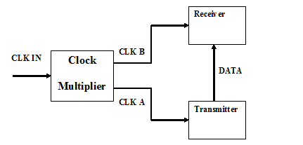
Figure 2.3 Common Clock Scheme
In common clock scheme, two clock cycles are required to complete a data transfer. In the first clock cycle (at the 1st clock edge of CLK IN) , at the edge of the CLK A, the Data comes out of the transmitter and propagates towards the receiver. On the second clock cycle (at the 2nd clock edge of CLK IN), the data latches in at the receiver.
This scheme puts some limitations on the lengths of the transmission lines of the clock signals and the data signal. Consider that you run a very long coaxial cable for the DATA signal from the transmitter to the receiver say 2 miles !!!. While the traces for CLK A and CLK B are small, say 2 inches. On the edge of the CLK A the transmitter gives out the DATA signal. The data signal starts traveling on the 2 miles long cable. While the data is still on the cable, the next clock edge of CLK B arrives at the receiver. The receiver now expects the data signal at the edge of the clock. But where is DATA? It is still traveling in the cable !! Chip designers express this by saying that the set up time of receiver is not met. In Synchronous clock scheme we should adjust the lengths of the CLK A, CLK B and DATA so that the setup time of the receiver is met. Few ways to improve the setup time margin could be reducing the length of the DATA signal and CLK A signal and increasing the length of the CLK B signal.
Now consider that your clock frequency is 100 MHz. This means that the time period of the clock cycle is 10 ns. Assume that Tom is designing a PCB. The size of the PCB is very huge. He kept the clock multiplier IC very close to the receiver IC (referring to the figure above). However, the transmitter IC is very far from the receiver IC. So far so that, the signal takes 12 ns from the clock IC to travel to the transmitter IC. Also the signal take 13 ns from the transmitter to the receiver IC. Now when the next clock edge arrives at the receiver IC, where is the DATA ?
Had we reduced the clock frequency to 10 MHz or cycle time to 100 ns, the receiver clock could have caught or toms DATA. Put in another way, the finite lengths of the clock and the data signals limit the maximum attainable frequency in the common clock scheme.
Common clock frequency scheme is adequate for the frequencies up to 200 MHz. The delay in the components clock to output time and PCB traces put an upper limit on the maximum allowable frequency of the common clock signal scheme.
In the Source Synchronous scheme, the transmitter IC sends the DATA signal followed after some delay, by the clock signal. The receiver latches the data signal on the edge of the clock signal. Using this scheme the bus speed is significantly increased as compared to the common clock scheme. Meeting the setup time requirement is a matter of relative adjustment of the CLK and DATA lengths as far as PCB design is concerned.
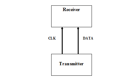
Figure 2.4 Source Synchronous clock scheme
2.5 Incident Clocking
Incident clocking is a kind of source synchronous clocking in which transmitter sends out the data and the clock signals simultaneously. There is no delay between the data signal and the clock signal. The receiver has a built in delay for the clock to meet the set up time requirements. If we keep the data and clocks synchronous and keep their lengths on PCB same, the two signals experience similar distortions in the path and the same amount of timing delays due to distortions.
Previous - Integrity of Point to Point Signal Next - Coupling of Traces