2.2 Time and Distance
CHAPTER 22.2 Time and Distance
Setup and hold time is useful for chip designers and simulation engineers. As PCB designers, we need to finally measure the things in terms of the length of the trace that travel on the PCB.
The electric signals are electromagnetic wave and their speed of propagation depends upon the dielectric constant of the material surrounding it. The Formula for the speed of propagation is
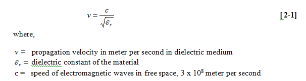
The speed of the electromagnetic wave in the free space is 3 x 10⁸ meter per second. The dielectric constant of free space is taken as 1. Let us say, the same signal propagates in a dielectric with a dielectric constant of 4, its speed will reduce to half or 1.5 x 10⁸ meter per second. We have already learnt this in High School Physics classes. In PCB designs we use another term propagation speed and measure it in terms of pico second per inch. The velocity of 3 x 10⁸ meter per second is equivalent to 84.7 pico second per inch.
A signal propagating in an inner layer, sandwiched between dielectric of dielectric constant of 4 will have a speed that is half of the free space propagation speed or 169.4 pico second per inch. What happens if a signal propagates in an outer layer? On one side we have a free air while on the other side we have a dielectric. The effective dielectric constant is smaller. The speed of the propagation will be somewhere in between that of the free air and that of the dielectric medium. We can take the help of calculators to find the speed of propagation.
As PCB designers, we will be required to match the flight time between a set of signals. If two signals travel both in outer layers, matching the flight time is same as matching their length. If however, one of the signals propagates in outer layer and the other signal propagates in inner layer, their speeds of propagation is different and matching the lengths will not ensure that their timing is matched. Let us consider one signal, say CLK, propagates in outer top layer, while the other signal, say DATA, propagates in inner layer. Since the DATA signal will propagate slow (being in inner layer), we will have to decrease the length of the DATA signal to match the flight time of the CLK signal.
The following example will explain the point.
Example 2.1 - IC A is the source of a clock and a data Signal. The IC B is the destination of the clock and the data signal. The clock signal is routed all on outer signal and has a length of 12 inches. The data signal is all routed on the inner signal. Find the length of the data signal to match the flight time of clock signal. Assume propagation speed on outer layer (microstrip) as 136 ps per inch and that in the inner layer (stripline) as 170 ps per inch.
Solution
[Note that the propagation speed is mentioned in picosecond per inch not inch per picosecond. We usually measure speeds of the cars in sort of inch per second ....]
Time taken by clock signal = Distance traveled by Clock x speed of clock signal
(in ps/inch)
= 12 inch x 136 ps /inch
= 1632 ps
Time taken by Data signal = Distance traveled by Data x speed of data signal ( in ps/inch) = Distance traveled by Data x 170 ps /inch
Now, since
Time taken by Data signal = Time taken by clock signal
=> Distance traveled by Data x 170 ps /inch = 1632 ps
=> Distance traveled by Data = 9.6 inch
As we have seen, we have to keep the distance of the data signal shorter.
In normal circumstances we would like to keep the matching signals in same layers. If however, we can not do that, we should calculate the flight time as in above example.
Previous - Integrity of Point to Point Signal Next - Coupling of Traces