What Causes EMI
From a PCB Designer point of view, we must understand the major causes of the radiated emission. Keeping ourselves aware of these issues will minimize the failures in EMI tests.
We will briefly review the major sources of the Electromagnetic Radiation in a typical design.
Cables
When a driver sends a current down a PCB trace, most of the returning signal current flows on the plane directly beneath the signal trace. However, in an attempt to find the minimum inductance path, some of the returning signal spread out over the plane. We call this stray current. When this signal, for example, crosses a via or an inter board connector, there is a change in returning current path by way of change in power plane. This sudden change leads to significant increase in the stray current. A cable carrying a current, similarly has a return path. If however, there is an current that does not return, it becomes a common mode current. Common mode currents radiate. Common mode currents in cables outside the box are most common sources of the EMI failures.
Field induced in cables
If there is a trace carrying high speed signal, it can induce the voltage in the trace in the nearby trace. If there is a cables attached to this trace is going out of the board, it can result in significant radiated emissions. This mechanism is illustrated in Figure below.
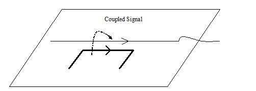
Figure - A high speed signal can induce current to a nearby conductor that may be going out of the board as an IO cable
All traces that go to a connector and having finite cable length out of the board must, therefore be kept away from high speed signals.
Clock Oscillators
Next to cables, Clock oscillators are major sources of EMI. Cycle after cycle clock oscillator send signals and superimpose upon each other. Observed on spectrum analyzers, these signals are observed as radiation. In most cases, the harmonics of these clock oscillators are also observed.
Mismatched Transmission Line
Transmission lines A mismatch transmission line will increase EMI. A matched transmission line will minimize it. Mismatch in transmission lines die to the via, layer change leads to increase in stray current. A matched transmission line reduces probability of radiation besides improving signal integrity.
Long Traces
High speed traces connecting clock and data lines are sources of radiation. The amount of the radiation will depend upon the length of the wires. Longer the traces, more is the chance of the radiation. In special cases, if these length are multiples of the certain frequencies, it can lead to resonance condition and source of radiation.
How to Reduce EMI
There are preventive as well as curative methods available at the hands of designers. Pay attention to the preventive methods during the design stages. As a real world engineer you should also be aware of the methods and patches that can be applied to a failing board to make it pass EMI test.
Match the Transmission Line and Termination
Transmission lines radiate. The amount of the radiation will depend upon several factors. This includes, return path discontinuities and stray current when changing the layer. A mismatched transmission line and mismatched termination increases the emission.
Use Short Clock Lengths where possible
Even if your board area is large, do not unnecessarily spread out components. Spreading out components, especially the high speed clock signals will lead to longer transmission lines and will tend to create more EMI.
Use Differential Signaling
In differential signaling , the two wires carry signals in opposite directions. One of the wires carries a current which is opposite to the direction of the current in the other wire.
The magnetic field generated by one wire has a direction opposite to that of the field generated by the other wire. Any radiation field generated by one of the two wires is canceled by the radiation field generated by the other wire. It essentially means that the radiation by a differential pair is substantially less.
To take advantage of the separation between the differential pair is as small as possible. If we increase the separation between the traces, then the antenna close to the positive pair will have more field strength due to the positive pair than to the negative pair. The result will be a net electric field and the resulting EMI. Therefore, the differential pair should be routed as close to each other as possible.
In order to take advantage of the radiation cancellation from differential signaling, the two signal pairs must be routed symmetrically and their length must match as close as possible. If their lengths are not equal or they are not routed symmetrically, the radiation pattern will not cancel completely.
Another factor we must keep in mind is that the common mode radiation created by the common mode currents in the two wires do not cancel rather they add up. Therefore there will not be any reduction in the radiated field due to the common mode current. We must however, note that creating any kind of imbalance in the differential pairs increases the common mode voltage and current and therefore increases the radiated emission.
Practically speaking, the differential signaling will improve EMI performance over the corresponding single ended signaling because of the fact that the common mode typical voltage level is far less than the corresponding minimum common mode level that would have been possible with the single ended signaling.
Use Higher value of Series Resistor
The amount of the radiation from a high speed trace will depend upon the amount of the current flowing in the trace. If we need to reduce the EMI, we should reduce the amount of the current flowing, especially, in the clock circuits. This can often be achieved by increasing the series resistance. Increasing the series resistance will decrease the current and thereby reduce the amount of the radiation. Another effect the series resistance has is that it dampens the signal which in turn reduces EMI. We must ensure through the simulation that the higher series resistance does not lead to the signal degradations.
Usually, increasing the series resistance will show a slightly dampened waveform at the receiver. Once you have carried out simulation for perfectly matching value of the series resistance, extent the simulation experiment for higher value of the series resistance. There will be ranges of values of the higher series resistance which will give the acceptable signal at the receiver. If you care about EMI, select a series resistance at slightly higher than the nominal value.
If you can, try to simulate not only for the voltage level at the receiver, but also the current waveform in the trace. Increase the series resistance and try to see if it leads to substantial decrease in the current amplitude without any substantial degradation of the voltage waveform at the receiver.
Use Stripline over Microstrip for Critical Nets
When a high speed signal is propagating, its electromagnetic fields are confined within the ground and power planes. In case of the microstrip the electromagnetic fields are confined between the trace and the return ground path. In case of the stripline, the electromagnetic fields are confined between the surfaces. Striplines, therefore radiate less than the microstrips. If there is a known clock net that seems to fail in EMI or is likely to fail EMI, it should be routed as stripline in place of microstrip. The electromagnetic waves are well contained within the ground and power planes in case of striplines and therefore there is at least some improvement over the corresponding microstrip structure. It is important that the we should consider other aspects of the design. Striplines do take up more space and there is more signal loss during propagation.
Board level Shielding
If the radiation can not be contained using all the novel methods, we must make a provision of shielding. There are many ways shielding can be achieved. If we know a particular area of the circuit that is found to radiate more than other areas then we can enclose that area of the PCB using metallic enclosures. As a PCB designer you should work in advance to make a place for fitting the mechanical enclosures. Most of the RF circuits have metallic enclosure not only to reduce EMI but also to keep it safe from external radiations.
Consider a project which has a very small life say nine months. The profit margin for the product is high. You do have a second chance to design, but you will loose a substantial amount of revenue. For such product, making a provision for metallic shield may make sense if the space allows.
Shielding should, however, be a secondary choice. Attempt should be made to make the non RF products pass EMI tests without the shielding.
Use Lower Voltage Swing
Higher the voltage level more is the current, more is the radiated emissions. Reducing the voltage level reduces the amount of the current flowing in the structures and therefore reduces the EMI. If you have a choice during the architecture stage of design, prefer the one that uses lower voltage levels to operate. If you have a clock oscillator and if you have a choice, use a lower voltage level to operate it.
Use of lower voltage also reduces the power consumption. If you reduce the voltage level by half, you reduce the power consumption by one fourth. If you are using external oscillators for your system you should be able to find different parts in the series operating at different voltages. You should choose the one that uses power supply lowest voltage, still being sufficient for your design.
As you lower the voltage swing your signal becomes more susceptible to noise. To overcome susceptibility to noise, you can use a differential signal, if your design allows. Otherwise keep the critical signal away from other high speed traces to make it less susceptible to cross talk noise.
Do not route Critical Signals near edges
All critical clock signals should not be routed at the edge of the Board. When the traces are routed in the inner section of PCB, the return signal flows mostly under the signal on the power planes. There is little, if any, stray current at the edges of the board. When the critical signals are routed at the edges of the board, the stray currents are at the edges of the board, resulting in more radiation.
Use of Metallic Shields or Enclosures
One of the ways for a equipment that would otherwise fail FCC test is to enclose it in metallic enclosure. Most of the personal computers will fail FCC test if they are not enclosed in a metallic enclosure. By using metallic shielding, the amount of radiation is reduced.
Metallic enclosure should not have gaps in between them to be most effective. Ideally they should not be any slots or holes. If there are slots or holes, they should be as small as possible. The thickness of the shield is of secondary importance.
At frequencies less than 100 MHz, you will need magnetic materials for the enclosures to be more effective. At higher frequencies the small openings will allow high frequency radiation to escape through the openings.
The designers sometimes make a provision for the metallic enclosure in the beginning of the design. Computational products with very high IO frequencies have more radiations and are more likely to fail in FCC tests. The metallic enclosures come at their rescue.
Shield Conductive Coating
In many cases, the plastic enclosure in place of metallic enclosure is decided to be used in the beginning of the design. If the equipment fails the FCC test, then metallic chemical coating can be used in the inner side of the plastic enclosure. A coating one to two mils thick can provide an attenuation of 20 dB or more. This should be sufficient to make most of the failing equipment to pass EMI test. Super Shield from MG Chemicals is one such product.
This is not to suggest that this method should be used as a general practice. In fact, as an electrical designer we must strive to design a product that does not need a shield coating or a metallic enclosure for that matter. The business requirement, however, may dictate that we do use them when we have no other choice.
Use of Spread Spectrum Oscillators
In the EMI analysis you will find that your equipment fails at a certain well defined frequency and its harmonics. If you trace the source of these oscillations, they may correspond to a particular oscillator. These oscillators have a well defined frequency. Observed in spectrum analyzers they will have a well defined peak amplitudes at a well defined frequencies.
One way to reduce the peak amplitude at the well defined frequency is to use spread spectrum oscillator. A frequency of spread spectrum oscillator varies back an forth around a nominal central frequency. The amplitude of both the fundamental and the harmonics is reduced by making the clock frequency vary in time. The energy remains constant, a varying frequency broadens the fundamental and harmonics and decreases their amplitudes.
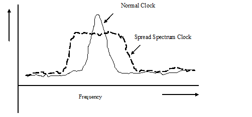
Figure Use of Spread Spectrum Oscillator for EMI control
Most of todays processors are designed too accept spread spectrum clocks. Increasing the amount of the spread reduces the spectral peaks.
Spread spectrum oscillators have inherent lower frequency jitters. Spread spectrum oscillators, therefore, can not be used in optical communication devices that need jitter free frequency reference.
FCC regulations are concerned only with peak emissions at any given frequency. A circuit designer can focus their EMI design efforts with reducing the peak emissions at any given frequency within the frequency spectrum, not the overall average emissions within the spectrum.
Spread-spectrum techniques are not meant to replace the EMI-reducing techniques of filtering, shielding, and good layout practice. As a design and signal integrity engineer our first priority is to have a proper PC-board layout. However, spread-spectrum clocks can aid EMI certification and quicken products launch to market while we go to the root cause in the next revisions. As a safety measure, the designer may use a footprint of a spread spectrum oscillator in design, just in case.
Previous Next