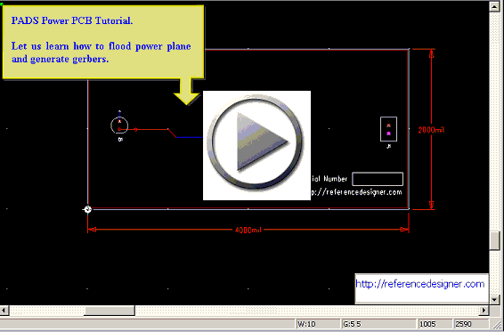
PADS POWERPCB TUTORIAL
Flooding Power Plane
We have used Power planes, however, we should flood them with copper before we generate the gerber. To do this Select Tools -> Pour Manager -> Plane Connect. Select both the layers and click Start.
This will flood the Mixed / Power Planes. We should now check for any connectivity error. TO do this go to Tools -> Verify Design -> Connectivity. Hit start. If there is any error it wil show up. You must recity the errors befor proceeding further.
A note on flooding -> Keep the file just before flooding saved and keep it a different name. It is often convinient to work on the un flodded board for any design change.
Gerber File Generation
We will now learn how to generate gerber files.
Click on file -> CAM. The minimal gerber files consist of the following
1. Four Routing Layers
2. Solder Mask for Top and Bottom
3. Silkscreen Files
4. Drill Drawing
5. NC Drill File
Click on Add. In the screen that follows - Under Document Type - Select Routing and Select Layer Association - Top Layer. Give a name to the Document, say, Routing - Top Layer.
Now hit the preview selection. You should be able to see a preview of the Top Routing Layer. Carefully examine to make sure that this is as expected.
Now click Layers. In the Selected, click Top. Under the Other, select Board Outline. If you click preview now, you should see a Board Outlline.
The standard practice includes creating a separate file for Board outline and not including it in Top or botom layers routing. However, this method is good for beginners as he can preview it and it works with all PCB vendors.
Cick ok and come back to the CAM Documents Screen. Repeat the same process for inner layer 2, inner layer 3 and the bottom layer. Do not incude board outline for inner layers.
This will complete the routing Layers CAMs.
We will now prepare to generate the Solder Mask gerber. Click on Add. In the screen that follows - Under Document Type - Select Solder Mask and Select Layer Association - Top Layer. Give a name to the Document, say, Solder Mask Top.
Now hit the preview selection. You should be able to see a preview of the Top Solder Mask Layer. Carefully examine to make sure that this is as expected.
Do the same thing for the bottom Solder Mask Layer. The next step is to prepare to generate the Silkscreen gerber. Click on Add. In the screen that follows - Under Document Type - Select Silkscreen and Select Layer Association - Top Layer. Give a name to the Document, say, Silkscreen Top.
Now hit the preview selection. You should be able to see a preview of the Top Solder Mask Layer. Carefully examine to make sure that this is as expected.
There are different ways the reference designation can be associated and displayed in Silkscreen. The only way to gaurantee that the things are good, is to see it in the preview. Make changes in the items in Top and Silkscreen layers, selecting and deselecting the items, till you get what you want.
You should also verify that the additional texts, logo, serial numbers appear in the Silkscreen as desired.
Repeat the same thing for the bottom layer. This completes the Silkscreen generation.
We will now prepare to generate the Drill Drawing. Click on Add. In the screen that follows - Under Document Type - Select Drill Drawing and Select Layer Association - Top Layer. Give a name to the Document, say, Drill Drawing.
Now hit the preview selection. You should be able to see a preview of the Drill Drawing. It has three parts - A drill drawing, a Drill Table and a Fabrication Drawing Notes. The Drill Table and the Drill drawing may have overlapping areas. To rectify this problem, click on the Options -> Drill Symbols -> change the X, Y location of the Drill Chart till you get them right. Use preview to view and make sure it looks good.
This will complete the Drill Drawing. Click on Add. In the screen that follows - Under Document Type - Select NC Drill. Give a name to the Document, say, NC Drill. Click OK.
We must now save the documents definitions. Now select all the Documents. Click on the Top Layer 1 and the while holding Shift click on the NC Drill. Now hit save.
We have still not generated the gerber files. To do that select all the Document Definitions and click run. This will generate the gerber files. These are usually placed in the directory C:\padspwr\CAM\default.
You may optionally generate a Aperture Report. Click Aperture Report on Define CAM documents. Give it a name in the screen that follows, say, aperture.rep. Click Save. This will generate the aperture report.
This completes the Gerber File generation. You may add a text file with details of you company name, contact details etc, before sending it to PCB manufacturer.
You can view the Flash of the above at
If you like this tutorial, you may like to get the book Signal Integrity for PCB Designers