PADS POWERPCB TUTORIAL
Modifying Silkscreen
The silkscreens go into separate layers. There will be two silkscreen layers, silkscreen top and silkscreen bottom. Before we modify the silk screen we will make the silkscreen layers visible.
Go to Setup -> Display Colors -> Browse down to Silkscreen top and Silk Screen Bottom. Tun the Line, Text, Ref. Des., and Outlines ( top and bottom) to, say, white color.
To move the reference designation choose the Design tool
 followed by "Move Reference Designation" button
  . If you click on the reference designation now, it will "lift" the reference designation and the component will get highlighted with yellow. Move the reference designation to the desire place. If you want, you can rotate the resference designation by Clicking "Control +R" on the fly.
You may also like to add company notes. Make sure that the current layer is Silkscreen Top. Click on the Drafting button
 followed by the Text button
  . Enter the desired text and place it at desired location.
Note that if you had not chosen the Top Silkscreen Layer, the text will go to the undesired location.
Automatic Board Dimensioning
We will now learn how to enter the automatic Board Dimensioning. Auto dimensioning is used to dispaly the board width and length.
Click Autodim button
 . With Select button
  highlighted, right click and select the "Board Outline". Now select the Horizontal Button
  . The purpose is to let the autodimensioning tool snap to the corner of the board outline. Now click on the two bottom corners of the board outline successively. The autodimensioning tool will automatically create dimension. Drag it to the place you desire and place the dimensions of the board.
Repeat the same same thing for the vertical dimension. Goback to the slect tool. Right click and select the Boad outline again. And then select the "Vertical" button
. The purpose is to let the autodimensioning tool snap to the corner of the board outline. Now click on the two bottom corners of the board outline successively. The autodimensioning tool will automatically create dimension. Drag it to the place you desire and place the dimensions of the board.
Repeat the same same thing for the vertical dimension. Goback to the slect tool. Right click and select the Boad outline again. And then select the "Vertical" button  . Now click the right two corners of the board. This will make the vertical dimensions.
Fabrication Drawing Notes
Fabrication drawing notes are the text and figures to give details of the PCB manufacturing. These are placed in the Drill Drawing Layer.
Before placing the Fabrication drawing make the Drill drawing layer visible. Go to "Select" -> Display Color -> Browse to "Drill Drawing" layer and mark Lines, Text, Outline to say, Red color. Click OK.
This completed the Reference Designation, Board Dimensioning and the Fabfrication Notes.
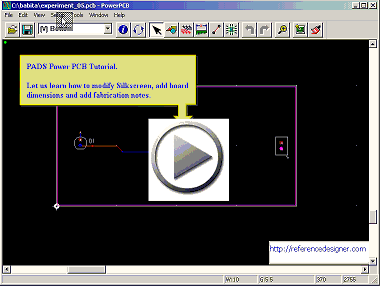
You can see tha above in a Flash movie in the following link.
We will be covering plane flooding, connectivity DRC check and the gerber generation in next.
If you like this tutorial, you may like to get the book Signal Integrity for PCB Designers