Allegro PCB Design Tutorial
The Design Object
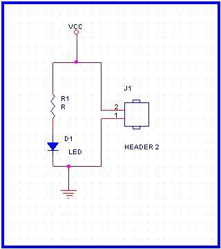
The purpose of this particular tutorial is to create a 4 Layer PCB for the following Circuit.
1. The Schematics has been drawn in Orcad. If you are not familiar with Orcad, you may like to take an Orcad tutorial.
2. Although this "simple circuit" can be done using a two layer board, we are making it 4 Layer board to understand the concepts of Power and Ground Layers.
3. As shown in the Schmatics, the circuit uses three components
R1
J1
D1
4. As far as the functionality is concerned the circuit is used to make an led D1 glow when a Power Supply is connected at the connector J1.
5. Each component will have an associated footprint. We have given the followintg name to the footprint of the components used.
| Component | Footprint Name |
| R1 | RES_SMT |
| J1 | HEADER2 |
| D1 | LED |
In the next few pages we will be creating padstacks and footprint before moving on to the layout.