Questions and Answers #2
Q13. Which of the following is NOT true about SSN ( Simultaneous Switching Noise)A. Faster IO edge rates generate more SSN.
B. Greater the number of data I/O pins, more is the SSN.
C. Smaller load capacitance increases SSN.
D. Higher package pin inductance increases SSN.
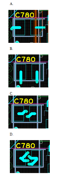
Q14. Consider the PCB traces for connecting the traces of a 1210 capacitor. Which of the following is the best way to connect the traces to power and ground pins for minimal trace inductance.
Q15. A transmission line has a small capacitive discontinuity along its length. It can be partially overcome by
A. Making traces slightly wider of at the two sides of the capacitive discontinuity.
B. Making traces thinner at the two sides of the capacitive discontinuity.
Q16. Consider a 50 ohm source driver driving a transmission line. The impedance of the transmission line is varied from 40 ohms to 60 Ohms in steps of 5 ohms and the following simulation curve is obtained. Which of these belong to 55 ohm
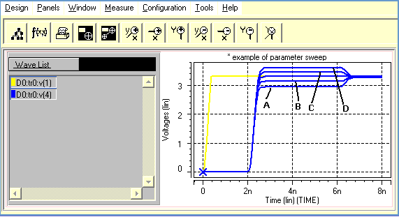
A. Curve marked A
B. Curve marked B
C. Curve marked C
D. Curve marked D
Q17. When a signal propagates down a transmission line, it is reflected by a lumped capacitor encountered in its path. Which of the following is not true
A. The magnitude of the reflected wave is higher if the rise time is shorter.
B. The reflected wave has polarity opposite to that of the incident signal.
C. The magnitude of the reflected wave is smaller if the impedance of the transmission line is high.
D. The rise time of the transmitted signal slows down.
Q18. Which of the following is not the reason for speed improvement of DDR2 over DDR
A. DDR2 has on die series termination, while DDR has motherboard series termination.
B. DDR2 has differential Data Strobe Signals (DQS) while DDR has single ended Data Strobe Signals (DQS).
C. DDR2 has smaller clock latency (CL) than the DDR
Q19. Assume a differential clock signal and a single ended data signal. If the length of differential clock signal is same as that of the data signal, then
A. The clock signal arrives earlier than the data signal
B. The data signal arrives earlier than the clock signal
C. The two signals arrive simultaneously.
Q20. Consider two signals A and B both having equal length on the PCB. The signal A is the DDR command and address signal and has more capacitive loading than that of signal B, a clock signal. A signal is launched simultaneously on trace A as well as trace B. Ignoring the fact that clock B is a differential signal,
A. Signal A arrives at its destination earlier that the signal B at its destination.
B. Signal B arrives at its destination earlier that the signal A at its destination.
C. Both the signals arrive simultaneously at their destination.
Q21. It is required to achieve 50 ohm impedance on a 2 Layer board which has bottom layer as the ground layer. Which of the following will achieve this with least thickness of the top layer trace.
A. Board thickness 0.063 , Er = 4.7
B. Board thickness 0.033 , Er = 4.7
C. Board thickness 0.063 , Er = 3.8
D. Board thickness 0.033 , Er = 3.8
Q22. Which of the following are not the advantages of the reduced voltage signaling
A. Reduced Power consumption
B. Reduced EMI
C. Less susceptible to noise
Q23. Which of the following is not the advantage of using a higher impedance (say 70 Ohm) over a lower impedance (say 40 Ohm)
A. Lower power consumption
B. Simplified design for connector and cables.
C. Reduced Cross talk
D. Better attenuation
Q24. Which of the following is not true about ISI
A. The ISI is higher if there is capacitive or other discontinuity in the signal path.
B. The ISI can be partially removed using pre-emphasis
C. ISI can not be observed using eye diagram
Previous Next