Miscellaneous SI Topics
Package ModelThe model of a complex IC will usually consist of two parts one is the model of the silicon itself and other is the model for the traces interconnecting the silicon to the pins of the package.
To understand package and the parasitics, take a look at the following IC picture. The picture is for an AMD processor. This particular processor is a multi-chip module which means that there are two silicons on a single package. The traces from the silicon cover a finite amount of trace when coming from silicon to the BGA pins of the IC. This path has parasitic element associated with it. IBIS models them as and RLC matrix.
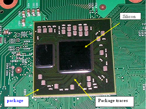
Figure - A processor IC showing silicon and package
A section of the IBIS model for the package looks as follows
<[Package]
variable        typ           min         max
R_pkg           0.17          0.07        0.33
L_pkg           1.95nH        1.15nH      3.12nH
C_pkg           0.52pF        0.29pF      0.87pF
With all its limitation, RLC matrix gives a good approximation for frequency components up to 1 GHz. Never omit it in your final simulation. The RLC matrix should also be used if you are trying to implement length matching for the positive and negative traces of very high speed differential signals. Ideally, we should calculate the difference in the electrical length of the positive and negative traces at the transmitter and the receiver in the silicon packages. This difference in the electrical length in packages should be balanced by the traces on the PCBs. If the trace length of the positive signal is higher than the negative signal in the silicon package then we should make the trace length of the positive trace in the PCB shorter. One drawback of this scheme is that the newer version of the package may have different lengths of the traces. Practically, the differences are very small and can be ignored.
Previous Next