Misc - Other topics
Consideration for Mixed PADs with and without ViasIn the design with BGA, it may be required that some BGA pins do not have the via in pad while others have the via in pad. For example the inner row pins will have the via in pad. The outer pins of the BGA are routed out of it and do not need via in pad.
It is required in such scenario, to keep the pad size of the pins without the via as close as possible to the pins with the via in pad. If there is a large difference in the sizes of the two pads, it will create a scenario where the height of the solder paste in the assembly process will be different because of the difference in the sizes of the land pattern. This will create the situation where the pads with different size will have different height of the solder paste. This may create an open circuit condition with the pad that has smaller height of solder paste.
PCB Designer should work with the assembly house on this issue prior to the release of the design to the PCB manufacturer if there is any doubt.
Blind Via and aspect ratio
Aspect ratio is for a blind via is defined as depth with respect to the hole size of the blind via. For example if the dielectric between the top layer and the second layer has a size 10 mils and blind via has a hole of size 8 mils then the aspect ratio is 10:8 or 1.25:1. The diameter of the hole should be large compared to the height of the hole or the laminate. In other words, small aspect ratio favors the manufacturing process. The designer should work with the PCB assembly house to find the aspect ratio allowed. For this reason, the one layer deep blind via will could easier to manufacture, than the two layer deep blind via. The aspect ratio will also be governed by the controlled impedance requirement as the height of the dielectric is one of the factors that determines the characteristic impedance.
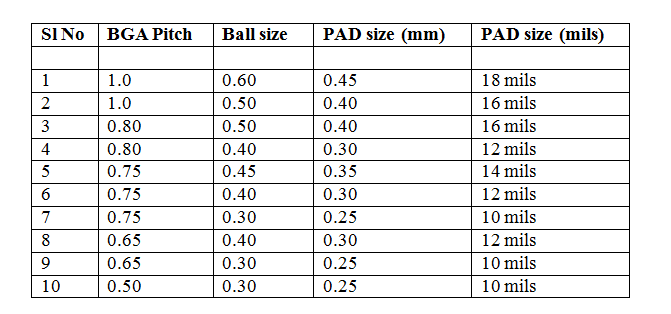
Relation between BGA pitch and pad size
The size of the PAD on the PCB for a BGA is governed mainly by the size of the BGA ball. You would like to pull out the datasheet of the BGA part and find the size of the ball. The PAD size will be slightly less than the ball size. For smaller BGA pitches, the pad size will be closer to the size of the pad. BGA pitch size is the distance between the adjacent balls of the BGA measured center to center.
You can use the following broad guidelines to find the diameter of BGA pads.
BGA pitch greater than 1mm gets 25% ball reduction. BGA pitch between 1 mm and 0.5 mm gets 20% ball reduction. BGA pitch less than 0.5mm gets 10% ball reduction.
The pads will also have mask which will have a diameter size approximately 4 mils greater than the size of the PAD diameter.
The table below gives the approximate size of the PAD for common BGA pitches and ball sizes.
Table - PCB Pad sized for give BGA pitch and ball sizes.
The IPC-7351A, Generic Requirements for Surface Mount Design and Land Pattern Standards also lays down the general guidance for the required sizes of the land pattern for a given BGA pitch and ball size.
The designer should make himself aware of the issues related to the use of the via in pad and blind via. If in doubt, the designer should creates a quick gerber around the BGA and send it out to the PCB Manufacturer for their recommendations. More often than not, the PCB house and the assembly house are able to help and recommend the best possible choice available.
Previous Next