Using Blind Vias in BGA based PCB Design
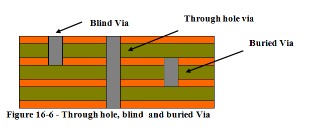
A blind via is a copper plated hole, that interconnects one external layer of the PCB with one or more internal layers, but does not go all the way through the board.A buried via is a copper plated hole that interconnects one or more internal layers, but does not connect to an external layer, hence the hole is completely internal or buried within the board.
The most compelling reason for the use of blind and buried via is that - it frees some PCB area that can be used for routing, thereby, saving board space. The blind via is used in conjunction with "via in pad" for fine pitch BGAs. Use of blind via is sometimes essential for fine pitch BGA component, where, using a through hole via is not an option due to space constraint. The use of blind via is more expensive than the traditional through hole via. The increase in the cost, because of the use of the blind via, sometimes compensates by way of reduction in layer count.
From signal integrity perspective, blind vias offer some added advantages. They have lower parasitic capacitance. For traces that have very fast edges, the blind via reduces the parasitic capacitance. If you have already used some blind via in your design for the BGA break out region, you should not hesitate to use it for signals too. You are not charged extra for using few more blind vias.
Previous Next