PCI Bus
PCI bus are still used in embedded systems. They dominated personal computers in 1990s and early 2000s. It is worthwhile to take a look at the signal integrity aspects of the PCI Bus.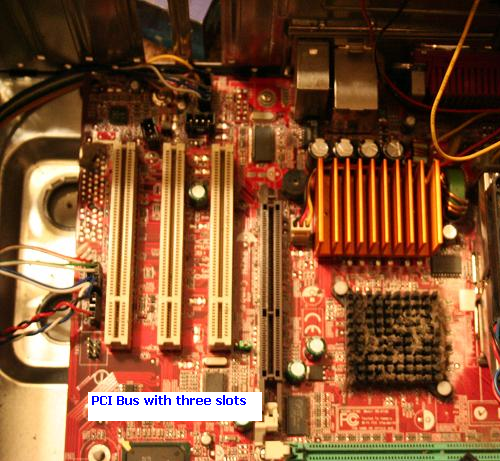
Figure - A PCI Bus with three PCI slots
Let us assume that in a PCI bus there are only two devices. The driver has a series resistance of 50 Ohm. When we say the driver has 50 Ohm series resistance what we mean is that the series resistance inside the driver IC pin plus the external resistor has is 50 Ohm. The driver IC will typically have 10 Ohm resistor. In that case the external resistor will have 40 Ohms value. We now have a 50 Ohm driver driving the 50 Ohm transmission line. Here is the sequence of events.
1. The driver sends a 3.3V signal.
2. According to the input acceptance equation we get a signal of half the size of the impressed signal on the transmission line. So a signal of 1.65V starts propagating along the transmission line. Note that if the transmission line impedance is higher, the signal impressed upon the transmission line will more than half. If the transmission line impedance is less than the driver impedance, the signal impressed will be less than half. It is all given by the equation
v2 = viZo/(Zo+Zs)
where Zo is the impedance of the transmission line.
Zs is the source impedance
vi is the amplitude of the impressed signal
3. Assuming the source impedance is same as the driver impedance, the 1/2 sized signal travels towards the load. There is no termination at the load. As a result, the half sized signal is completely reflected by the receiver. That is why PCI Bus is called reflected wave Bus.
4. The half sized signal starts traveling back to the source. Since the impedance of the source is matched to the transmission line, the signal is completely absorbed here.
5. The receive end sees a signal that is double to that of the half sized signal. The receiver, therefore, sees a full size signal. The signal transmission is stabilized when the reflected signal reaches the transmitter and completes one round trip.
The PCI Bus with only two device is very simple. This kind of signaling is often used in clocks. PCI Bus is however designed for multiple devices.
Consider now a driver with two traces coming out of it in parallel. The characteristic impedance of each of the line is 50 Ohm. Also assume that the lengths of the two lines are equal. The driver now see an impedance of 25 Ohm. To match this we make the driver impedance equal to 25 Ohms.
Let us now assume that the driver sends a signal. What we'll do is divide the 25-line in half, lengthwise. Split it into two parallel lines, each having an impedance of 50 ohms. From the driver point of view, it sees an impedance equal to its drive impedance. So it sends out a signal with amplitude one half the size of its amplitude. The half sized signal travel in both the transmission lines. These are reflected back from the two receivers. If the lengths of the two transmission lines are equal they are absorbed at the driver end.
Practical embedded system with PCI master and two PCI devices can use a routing strategy where driver is at the center and two PCI devices are at the left and right ends of the Center.
The computer systems have many PCI slots. A typical PCI based motherboard can have 3 or 5 PCI Slots. These slots are in series. The common topology that is practical from routing perspective is that they are routed in series one after the other. A card can be plugged in any of the slots. If a card is plugged in say first slot, it "loads" the bus and reduces its impedance and also introduces the discontinuity. In such case, a driver impedance slightly lower than 50 is probably a better match. We should also note that in case not intermediate card is loaded and only the end card would have been loaded, a 50 Ohm driver impedance would still have been the best match. So what we do ? Do we select a 50 Ohm driver impedance ? Should we select smaller drive impedance. There is no fixed answer. If we do select an impedance lower than the transmission line impedance, the reflected wave is not completely absorbed when it travels back to driver. We should simulate various conditions. Three common configuration that we must simulate for are 1. All the cards are loaded 2. Only end card is loaded. Only 1st card is load. This process should give us an idea as to what value should be a best fit. Once we choose a value we should simulate across all combinations to make sure that the timing and other specifications are met under all conditions.
It turns out that not all the energy is absorbed in one round trip. It make take 2 or 3 trips before the reflected signal dies down reasonably. Few things help in that process. One is keeping the traces short. This allow more round trips possible and allows more settling time before the timing window for data starts. Another thing that helps is having a device at the end of the PCI chain. If you have to put on PCI device on the board keep it in the end, rather than in the middle.
PCI architecture is not a purist delight. It is practical. It serves the purpose of flexibility. It works.
Previous Next