Miscellaneous SI Topics -Via
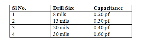
Similar to the right angle bend, many signal integrity engineers like to avoid the via in design. Vias are used to change the layers. As soon as we change layer, the new layer is bound to have some change in impedance. Even if you specify 50 ohms for two layers, because of the manufacturing process, the two layers will have slightly different impedance. As the signal travels from one layer to another, it sees some change in impedance. This leads to reflection and signal degradation.The via, in itself is capacitive. Addition of via is equivalent to addition of a lumped capacitance. However, the value of the via capacitance for small drill sizes, typically used in multilayer PCB design is very small. The table below shows the typical value of the capacitances for vias of different sizes.
Table - Typical via capacitance
Simulation must be performed to see the effect of the via on signal quality.
Previous Next