Miscellaneous SI Topics - Right Angle PCB Bend
I have seen a number of times when the design rule handed over by signal integrity engineer contains a line Avoid right angle bends. There have been two groups of engineers those who say right angle is allowed, and those who say right angle is not allowed. We will briefly examine the case for and against the right angle bend.The figure below shows a right angle bend created in a PCB trace. If you examine the outer edge of the right angle bend, you will notice that there is an increase in the effective area of the trace near the bend. This increase in the trace width results in increase in the capacitance near the bend. This results in reduced impedance near the bend.
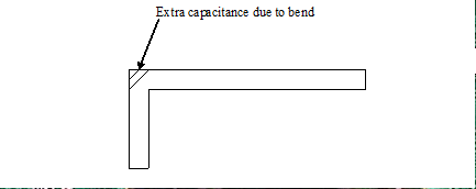
Figure - A right angle bend.
Time domain reflectometry (TDR) can be used to estimate the magnitude of the reflection and the corresponding additional equivalent parasitic capacitance introduced by the right angle bend. Experiments have been carried out and the result shows negligible capacitive reflection.
The bend does increase the capacitance. However, the dimensions are so small that, we can effectively ignore the reflections caused by the right angle bend. The PCB designers mostly use a 135 degree bend mostly in place of 90 degree bend. But the reason should not be the signal integrity. The reason is saving the routing space.
If bend is the cause of the increase in capacitance, let us calculate it. In the Figure below, draw a quarter circle with inner corner as the center and the width of the trace as radius.
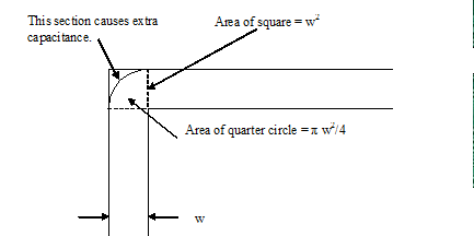
Figure - Calculating the Capacitance of extra part in Right Angle bend.
Now, we can assume that the width of the trace remains constant if we remove the area of the trace outside the arc. The area outside the arc represents the extra capacitance.
If w is the width of the trace, the area of the removed part is given by
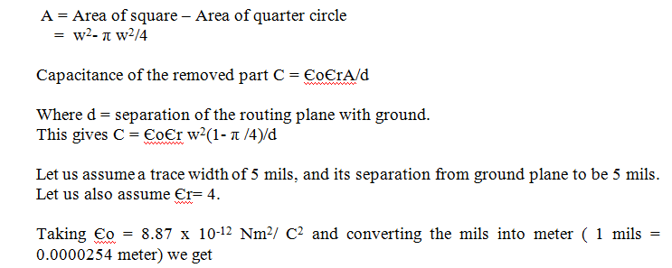
C = 0.01 pf
A typical value of 0.01 pf is too small a value to be considered a parasitic capacitor.
Previous Next